
The electronic and semiconductor industry is constantly evolving, bringing about new and powerful technologies at an incredible pace. One such emerging technology that promises to revolutionize chip design is 3D integrated circuits (3D ICs). As chip densities continue to increase according to Moore’s Law, 3D ICs present an innovative solution to circumvent many challenges of traditional planar chip design and help keep Moore’s Law alive for years to come.
What are 3D ICs?
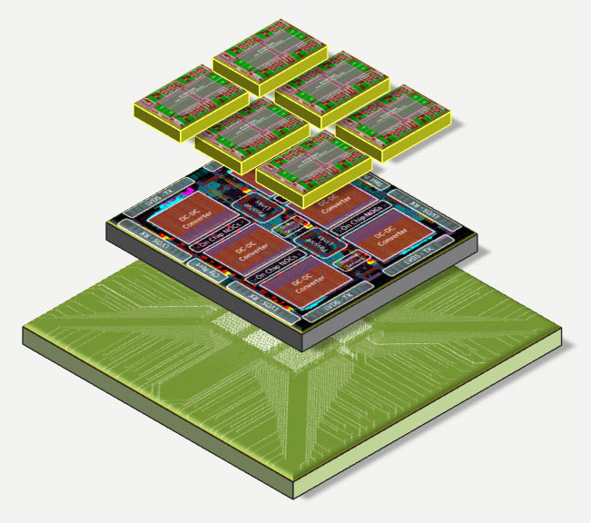
Traditionally, integrated circuits have been designed and manufactured on a single silicon wafer or die in a two-dimensional planar layout. In 3D ICs, two or more layers of active electronic components are vertically integrated and interconnected using wafer-to-wafer, die-to-wafer or die-to-die stacking techniques. This allows for a third dimension to be utilized for chip space. Several silicon wafers or dies are stacked on top of each other and through-silicon vias (TSVs) enable vertical electrical connections between the stacked layers.
Key advantages of 3D ICs
The major benefits of 3D IC design stem from the ability to utilize the extra dimension of vertical space. Some key advantages 3D ICs offer over conventional planar chips include:
Higher transistor density and performance – 3D ICs can pack significantly more transistors in the same footprint by using multiple layers of silicon. This improves computational power and performance. It has been estimated that 3D designs can achieve up to 10X higher transistor density compared to planar chips.
Smaller form factor and lighter weight – With their ability to miniaturize components using vertical stacking, 3D ICs take up less board space and are more energy efficient. This makes them ideal for use in mobile applications requiring compact designs.
Reduced power consumption and heat generation – Shorter interconnect lengths in a 3D design help lower resistance-capacitance delay products improving speed while cutting down power needs. Better thermal management is also possible.
Heterogeneous integration – 3D designs facilitate the combination of logic, analog, memory and other components onto the same chip. This allows for specialized system-on-chip solutions.
Increased design flexibility – Individual silicon layers can be fabricated independently using different chip technologies like FinFET, FDSOI, thereby boosting design versatility.
Complex 3D architectures – Advanced 3D designs with multi-layer stacks will enable novel architectures such as 3D network-on-chip. This can revolutionize on-chip communication.
Developments in the 3D IC Ecosystem
Considerable research efforts over the past decade have focused on developing the processes, materials and design methods needed for commercialization of 3D ICs. Some notable achievements include:
– Improved heterogeneous TSV fabrication using processes like via-middle and via-last that minimize stress and defects. TSV sizes under 10μm are now possible.
– Advanced stacking techniques allowing tighter pitch between layers with alignment accuracies below 10μm. Methods like thermal compression bonding are becoming mainstream.
– New low temperature bonding materials as alternatives to polymer adhesive die attach for thermally and electrically robust interlayer connections.
– Modeling and optimization tools to enable thermal, power and signal integrity analysis of 3D designs early in the development cycle.
– Maturing of design automation flows to support full-flow 3D Electronic Design Automation from placement to routing across multiple tiers.
– Demonstrations of advanced 3D prototypes for AI/ML accelerators, memory cubes and sensor fusion applications showcasing the technology’s potential.
Global industry leaders like Intel, Samsung, TSMC and SK Hynix have significantly scaled up their investments in 3D IC R&D focusing on chiplet-based modular designs and post-silicon interconnect innovation. Ecosystem players too are enhancing support for 3D-specific design/analysis needs. Major foundries can now provide prototyping runs for early 3D designs.
Applications and Future Potential
Going forward, 3D ICs are expected to find widespread usage across diverse chip applications:
– Memory: 3D multilayer DRAM and flash memory stacks can deliver game-changing density and economics for applications in data centers, smartphones and autonomous vehicles.
– Mobile SoCs: Advanced 3D mobile SoCs with powerful heterogeneous capabilities embedded in compact stacked footprint can enhance user experiences across new AR/VR product categories.
– HPC: 3D designs are critical to the packaging needs of next-gen AI processors and exascale supercomputers dealing with monumental data volumes.
– IoT: 3D sensors with vertically integrated photodiodes, processing elements and flash storage promise to revolutionize slim and long-lasting edge devices.
– Automotive: Complex 3D IC solutions for advanced driver-assistance and fully self-driving vehicles will aid the vision of safer mobility.
Looking ahead, 3D chip manufacturing is projected to become mainstream by the late 2020s with over 30% of total annual IC sales adopting 3D integration. Multi-tier 3D ICs with 5-10 active layers and beyond could emerge as the dominant backend IC packaging methodology. The combined benefits of density, performance and form factor will cement 3D ICs’ role in extending Moore’s Law to deliver unprecedented levels of system capabilities in the years to come. Undoubtedly, this groundbreaking technology heralds the future of silicon.
*Note:
1. Source: Coherent Market Insights, Public sources, Desk research
2. We have leveraged AI tools to mine information and compile it